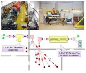
RBI Tandem Accelerator Facility

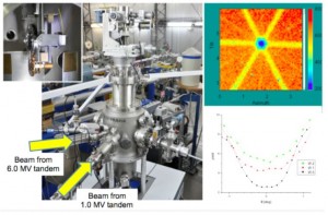
Dual beam & channeling end-station

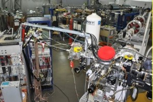
Ion microprobe
Materials modification using swift heavy ions is important contemporary topic in the field of applied physics. Such projectiles generate intense electronic excitation along their trajectory because at these kinetic energies (10-1000 MeV) dominant channel for energy dissipation is via numerous collisions with electrons in the material. Density of deposited energy is often quite sufficient to activate various thermally driven processes enabling patterning or synthesis of nano-structured materials. Interaction of swift heavy ions with material can result in formation of ion tracks and surface features (nano-hillocks or nano-craters) which can be found on the place of ion impact by means of scanning probe microscopy. Applications related to the nanoscale patterning of the crystalline material using swift heavy ions have already been proposed. Also, many questions related to our basic understanding of the underlying processes are still open.
Nuclear stopping causes various radiation damages to target materials such as sputtering, defect formation, and plastic deformation. Considerable efforts have been devoted to understanding of fundamental mechanisms relevant to irradiation effects in a variety of solid materials involving metals, semiconductors and insulators. Ion irradiation may transform crystalline materials into either a fully or partially amorphous state. Studies of ion irradiation effects on materials have recently received considerable attention and a great deal of effort has been devoted to elucidation of radiation damage. Radiation damage is natural phenomenon with sources like cosmic radiation or decay of isotopes in terrestrial rocks. Also, a variety of radiation sources are created and used in science and technology.
The problem of resistance to radiation damage is common in many areas. Also, ion doping can beneficially alter a material’s semiconductor properties. On the other hand, the inevitably accompanied structural alteration, if significant, is unwanted, and is therefore referred to as ‘‘radiation damage’’. Consequently, semiconductors resistant to radiation damage have important advantages, and are widely studied. Materials destined for use in hostile environments (high radiation doses, high temperatures …) such as nuclear (fission and fusion) reactors or waste immobilization, high-energy physics experimental devices (like at CERN) must be highly durable and especially resistant to radiation damage effects. Regarding high-energy physics experimental devices, new detector materials are under investigation, like for example diamond or SiC instead of silicon. Although there are experimental evidences that diamond based detectors would be more radiation resistive at GeV particle energies, the recent experiments show that it is probably not the case at lower energies (in MeV range). However, in the case of diamond and due to its unique properties, application perspectives are much wider when comapared to silicon. For example, ultra thin membrane detectors are used for radiation in-air windows providing trigger signal, microdosimetry for hadron therapy, creation of NV centers by single ion implantation in diamond for quantum computing developments. Knowledge about the radiation hardness of diamond and similar materials (SiC) is absolutely crucial in this respect.
Most studies on ion irradiation effects have focused on how the radiation defect causes a change in material properties and structural modification of materials. In most experimental studies, structure and physical properties of materials before and after ion irradiation are measured and examined within a framework of projectile energy loss consideration. This is because the energy loss of projectile ions is a key-parameter characterizing radiation effects. It is generally accepted that the energy deposition into a target, via nuclear (recoiling of atoms) and electronic (excitation and ionization) processes, transforms eventually to lattice vibration (heat) and radiation effects are induced during this energy-transforming process. Thus, actual situations relevant to energy transfer and its relaxation are complicated dynamical processes both in time and space. New approaches such as studying the time evolutions of radiation damages or their in situ observation have been extensively explored in recent investigations.
The RBI Tandem accelerator facility consists of a 6MV Tandem Van de Graaff accelerator and a 1MV Tandetron accelerator with a number of experimental end-stations. The facility is relatively well equipped for nuclear analytical measurements in interdisciplinary studies. The accelerators are capable to deliver a wide range of ions, with energies from about 100 keV to tens of MeVs, to eight beam lines. The beam lines in use are equipped with several specialized end stations for ion beam analysis (IBA) and ion beam modification studies, including IBA techniques such as PIXE (Particle Induced X-Ray Emission), PIGE (Particle Induced Gamma-Ray Emission), RBS (Rutherford Backscattering Spectrometry), TOF-ERDA (Time of Flight Elastic Detection Recoil Analysis), NRA (Nuclear Reaction Analysis), IBIC (Ion Beam Induced Current) and TRIBIC (Time Resolved IBIC). Focused ion beams can be obtained at the ion microbeam, and the dual beam end station is installed for IBA and ion beam modification studies. This last end station can be used to irradiate materials by simultaneously with two ion beams. Therefore in-situ irradiation and consequent diagnostics by two independent ion beams can be performed. One of the ion beams can be used for materials modification (damaging beam), while the second ion beam can be used for in-situ characterisation of induced changes (probing beam). This will be exploited by the project. In some cases, like for radiation damage research of the materials for nuclear power (fission and fusion related materials research) irradiation of the material with two different ion beams (like self-ions and helium beams) could be advantageous. We will also exploit the fact that this end-station is equipped with the goniometer stage, enabling RBS experiments in the channeling mode (RBS/c).
